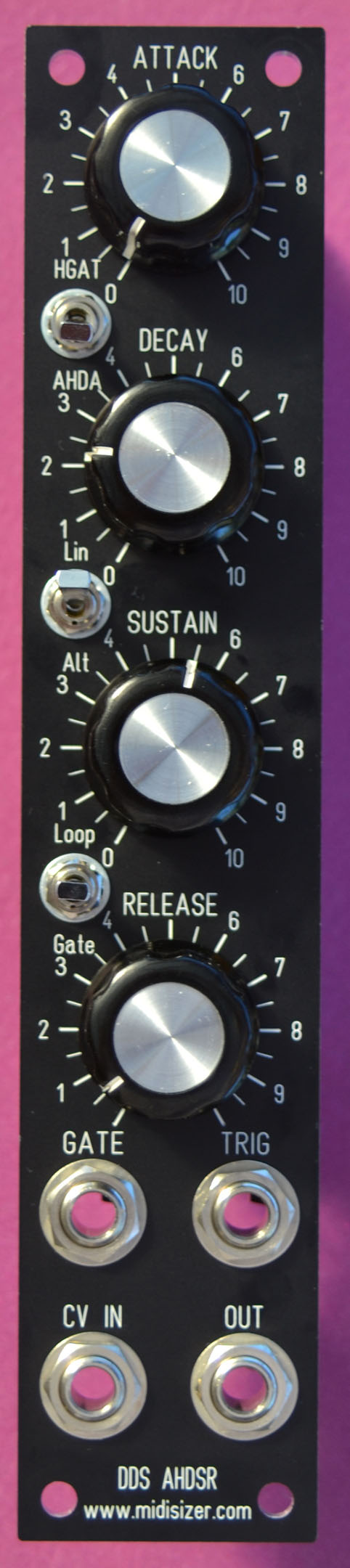
The DDS AHDSR is a compact yet versatile envelope generator module designed for 5U systems. Besides the classic AHDSR envelope mode with internal Gate length selection (a ’la KORG MS-20), envelope amplitude and Decay/Release time CV modulation, the module also has a convenient AHD mode with envelope amplitude modulation, contiguous and gated Cycle mode. In both modes envelope curves can be standard Expo, Linear or Logarithmic.
Here’s a video that demonstrates some of DDS AHDSR envelopes:
Production PCBs:

Controls
Function of the 4 knobs depends on the Switch 1 position:
Center
- attack time
- decay time
- sustain level
- release time
Up (HGAT)
- hold time
- gate time
- envelope amplitude modulation by CV
- decay/release time modulation by CV
Down (AHDA):
- attack time
- hold time
- decay time
- envelope amount modulation by CV
Switch 2
Controls envelope curve: exponential, linear and logarithmic.
Switch 3
Controls repeated mode: none, gated and contiguous.
Connections
GATE: note gate signal
TRIG: inverted note trigger signal
CV: control voltage input for envelope amplitude and Decay/Release time modulation
OUT: output control voltage
Technical characteristics
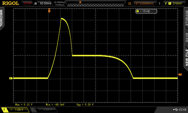
Envelope stage time: 1ms to 12 seconds
Input GATE/TRIG voltage: 0-5V or more
Input CV voltage: 0-5V
Output CV voltage: 0-5V (0-10V or -5+5V jumper selectable)
Power supply: +-12V or +-15V
Power supply current: +30mA/-5mA
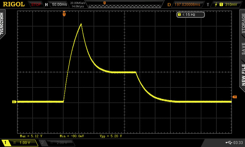
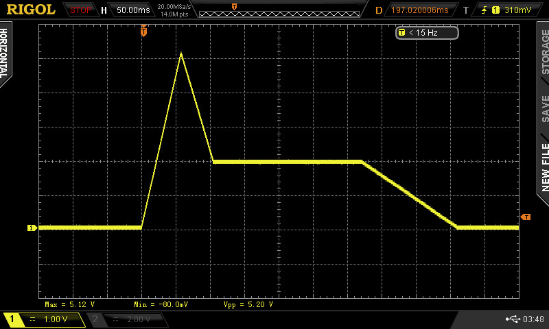
Envelopes
Standard exponential:
Linear:
Logarithmic:
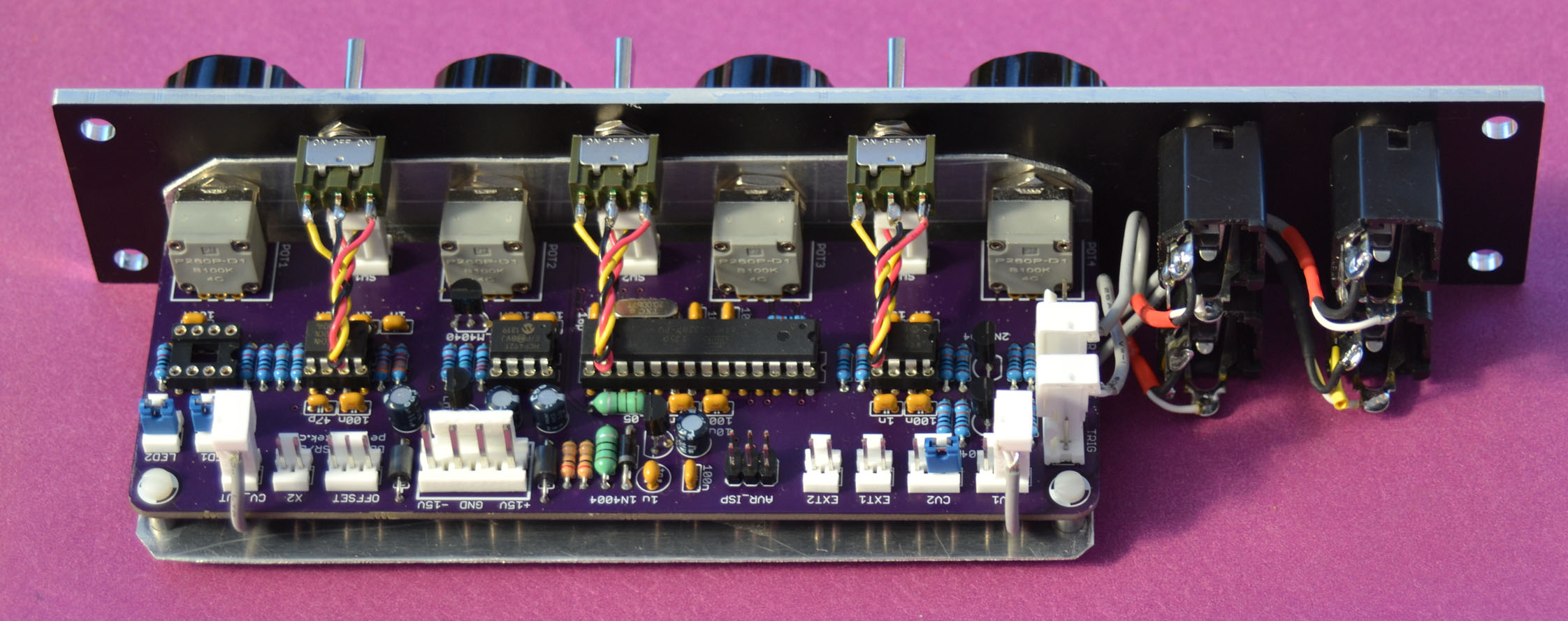
PCB description
The PCB is designed with some extras so that it could also be used for an advanced LFO project. For this reason it has one extra CV modulation input and two output LEDs, one for GATE and one for CV OUTPUT, both working in op amp feedback circuit to prevent clicking.
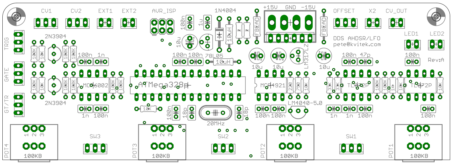
GATE: gate jack connector, normalled to ground
TRIG: trigger jack connector, normalled to +5V
GT/TR: gate and trig signals connector for chaining other AHDSR boards
CV1: primary CV input connector
CV2: secondary CV input connector
EXT1: first extension I/O port connector connected to PD0 (RXD) and LED op amp 1 input
EXT2: second extension I/O port connector connected to PD1 (TXD)
AVR_ISP: microcontroller flash programmer connector
+15V/GND/-15V: power connector (MOTM/Euro)
OFFSET: adding a jumper to this connector will offset output signal by -5V (for -5/+5V operation)
X2: adding a jumper to this connector will multiply output signal by 2 (for 0-10V operation)
CV_OUT: envelope CV output jack connector
LED1: first LED connector to blink with the GATE signal (optional)
LED2: second LED connector to blink with the CV OUT signal (optional)
DIY Resources
Schematics: xmod_sch
Eagle files: pcb_adsr
Firmware: xadsr_hex
Firmware source code: src_adsr
Front panel: xadsr_fpd
Ordering
To order DDS AHDSR, please send an email to pete at kvitek c o m specifying how many PCBs and pre-programmed MCUs you need, a country where to ship them, and an email address to send the PayPal invoice to.
Prices (US dollars):
- DDS AHDSR pcb $20
- Pre-programmed ATMega328p $10
California residents add 8.75% tax
Shipping:
- Continental USA — $5
- Canada – $10
- Europe, Asia and Australia – $15
Please make sure your PayPal shipping address is correct!
Acknowledgements
This project was inspired by Electric Druid’s excellent VCADSR project and was built using Mutable Instruments wonderful AVR programming framework Avril. Front panel is created using Modular Synthesis 1U basic panel template.

Pingback: 5U DDS AHDSR/AHD envelope generator | MidiSizer
Hi Peter,
Thank you for sharing your schematics, they are very helpful! If I understand correctly, in order to get a 10Vpp signal, you used the X2 jumper that’s bypassing the 100k. But the DAC has an option to have a gain of 2, I’m curious to know why you preferred your solution over this one?
Thank you,
Gregory
DAC output multiplier is not applicable here since the DAC reference voltage cannot be 10pp.
If I look at the datasheet, from what I understand, Vref doesn’t change. Let’s keep Vref at 5V, and then G is the gain selection, you can choose a gain of 1 or 2. With G=1, one gets 5Vpp, with a gain of 2, one gets 10Vpp.
Vout=Vref*G*D/4096
Am I wrong?
If the IC’s power supply is 5V where the DAC will get 10V from? If Vref is 5V and gain is set to 2, the output voltage will reach it’s maximum of 5V at 2048 then stop increasing because it cannot go above power supply voltage.
Ok, got it!
Thank you!
Gregory
hi peter, thanks for sharing this, a question about jacks connections: in trig e gate the switch goes to resistor, the tip to vcc e gnd to gnd? the same in cv’s? i’m a bit confused!
The XMOD PCB is designed to be universal, so on board gate and trig connectors provide both GND and VCC signals that can be used for normalization.
AHDSR firmware assumes all GATE and TRIG inputs to be normalled to GND, so please ignore VCC pin.
2LFO firmware does the same, I think.
BTW, if you decide to normal any input to VCC for some reason, please do so through 10K resistor soldered directly to the connector.